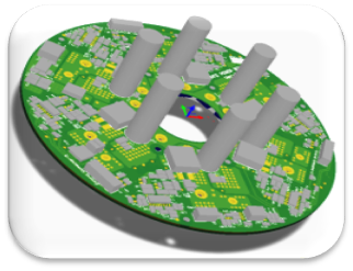
PCB Design
- Strategic placement of Magnetics, IC’s and Semiconductor devices
- Compactness to save board real estate
- Design for manufacturability
- Layout practices that ensure EMI/EMC compliance
- Multilayer PCB’s
Almost any and every power electronics engineer would’ve faced the brunt of a poor layout atleast once (if not more) in a design process.
Some of the essential steps in a good layout are
Innerve understands these constraints and helps its customers in a well designed PCB layout services.
Hands-on expertise in PCB design tools like ALTIUM, ORCAD and KiCAD(open source) make it easy for our customers and reduces the tools migration efforts